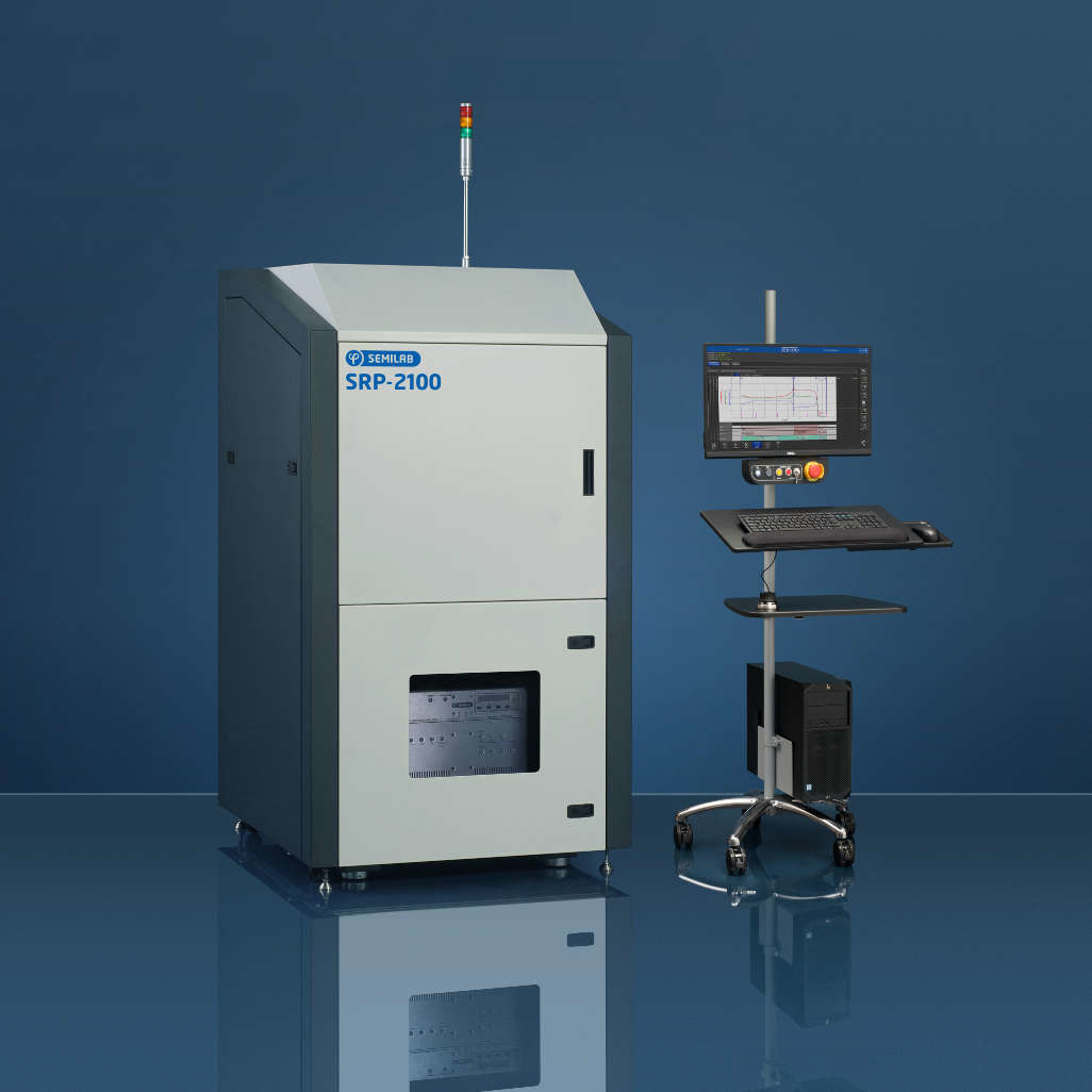
SRP-2100 Spreading Resistance Profiler
Explore the entire carrier density and resistivity profile in all silicon semiconductor structures of device processing with this automated system. Measurement range covers state-of-the art application needs.
Measured parameters
- Dopant concentration and resistivity
- Carrier density and resistivity profile shape
- Junction depth
- Transition width
- Sheet resistance
- Electrically activated dose
- Bevel Angle Measurement (BAM)
Features
- Ultrawide measurement range, flexible application
- High-resolution, non-overlapping measurement
- Transition zone, junction depth calculation
- In-Situ Bevel Angle Measurement (BAM)
- Low noise, ultrahigh precision stage
- Effective, high quality vibration and acoustic isolation in measurement chamber
- Touch-driven user interface and user-friendly software
Options
- P/N tester: dope and type characterisation by hot probe technique
- Shallow Layer Measurement (SLM): extending the SRP technique to determine thin layer structure
- Variable Probe Spacing (VPS): based on motorized probe spacing movement allows the measurement of sheet resistance of thin isolated layers
- Temperature Controlled Measurement Chamber (TCM)
- Signal Tower: standard industrial signal tower which gives information on system status
- Stand-Alone Bevel sample polishing unit


