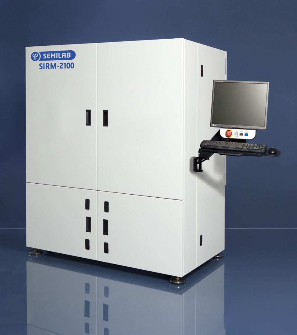
SIRM-2100, SIRM-2500, SIRM-3000
The SIRM Bulk Microdefect Microanalyzers are non-contact and non-destructive optical instruments, which provide a complete characterization of bulk microdefects (BMDs), such as oxygen and metal precipitates, voids, stacking faults, slip lines, dislocations in the bulk and in the near-surface region of the semiconductor wafers.
Features and System Specifications:
- Non-contact, non-destructive analysis
- No sample preparation is needed
- Image collection in X-Y and X-Z planes
- Measurement of epi wafers
- Detectable particle size: down to 30 nm
- Principle of operation: brightfield confocal scanning microscopy
- Measurement depth: approximately 200 μm
- Depth resolution in Si: approximately 5 μm
- Detection limits for defect density: 108-1010/cm3
- Mapping areas: 200 × 200 μm
- Depth range: 10 - 300 μm
- Depth resolution: 5 μm
- Lateral resolution: 0.4 μm
- Image size: 512 × 512 pixel
- Throughput: 60 sec/image
- Versatile evaluation software: automatic defect finding, exclusion, background correction
- From acquired data can be generated a database friendly file, which contains all the setting and evaluation results
- 300 mm wafer handling with automatic wafer recognition vision system
| SIRM-2100 | SIRM-2500 | SIRM-3000 | |
|---|---|---|---|
| Loading | Manual | Automated, 1FOUP | Automated, 2FOUPs |
Options:
- Wafer handler: single cassette up to 300 mm wafer
- Defect position marking
- CCD camera
- Dual laser with user-defined wavelengths
BMD characterization:
- Denuded zone determination
- Stacking fault
- Dislocations
- Metal precipitation
Request Info


