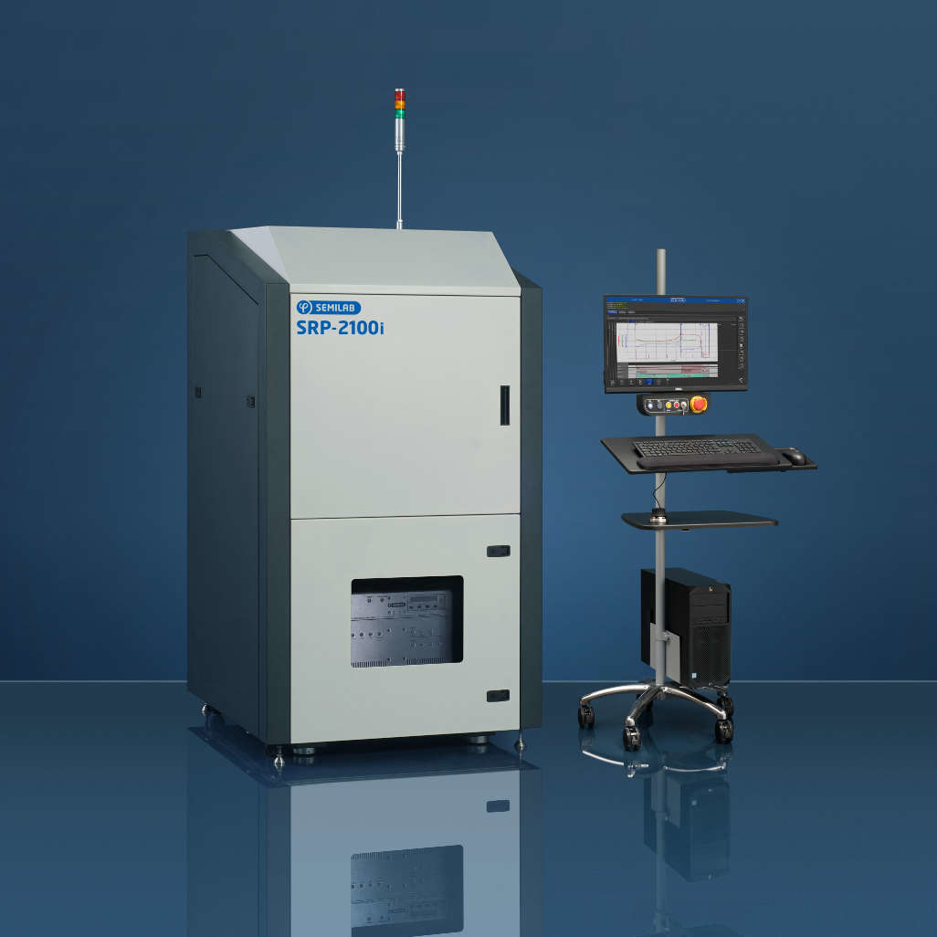
SRP-2100i Spreading Resistance Profiler with I-V capability
Explore the structure determination and profile monitoring of compound semiconductors and measurement of resistivity and carrier density profiles in all silicon semiconductor structures of device processing with this automated system. Measurement range covers state-of-the art application needs.
Measured parameters
- Dopant concentration and resistivity on Si materials
- Carrier density and resistivity profile shape
- Resistance profile on compound semiconductors: AlGaAs, GaAs, GaN, Ga2O3, InP, SiC
- AlGaN/GaN HEMT structures
- Junction depth
- Transition width
- Sheet resistance
- Electrically activated dose
- Bevel Angle Measurement (BAM)
Features
- Ultrawide measurement range, flexible application
- High resolution, non-overlapping measurement
- Transition zone, junction depth calculation
- In-Situ Bevel Angle Measurement (BAM)
- Ready to upgrade with PCIV option
- Low noise, ultrahigh precision stage
- Effective, high quality vibration and acoustic isolation
- Touch-driven user interface and user-friendly software
Options
- PCIV option for wide bandgap and SOI application: combines variable measurement bias and current-voltage curve analysis to measure spreading resistance profile on novel semiconductor materials
- Iterative PCIV software option (iPCIV): designed to measure highly variable samples with very high resistance value (ideal below 1E-11 A current range)
- Shallow Layer Measurement (SLM): extending the SRP technique to determine thin layer structure
- Variable Probe Spacing (VPS): motorized probe spacing movement allows the measurement of sheet resistance of thin isolated layers
- Temperature Controlled Measurement Chamber (TCM)
- Signal Tower: standard industrial signal tower which gives information on system status
- Stand-Alone Bevel sample polishing unit


